OUR PROCESSOR
We created a multicore processor with the intent of parallelizing program execution and allowing for optimized computing units.
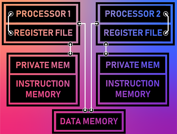
Using two of the same core computing units in a computer, we created a homogeneous multicore processor. Each of the cores has a private memory space, or scratch space, which is used for core-specific data storage as well as for instructions.
Our current implementation takes the sum of two core results. Both cores perform additions in parallel. Then, one core retrieves the result computed by the other core, sums it with its own result, and stores the final result.
MOTIVATION
Many modern processors have increased performance by adding cores to their architecture. The types of processors that have used this method for increasing performance range from processors used in desktops and laptops to the processors in phones. It is interesting to consider the areas in which improvements are made through multiple cores. By adding homogeneous cores, you allow for performance increases through multithreading and allowing computations to be performed on separate hardware.
However, you can also add heterogeneous cores to a processor. In this case, cores could be optimized for specific tasks. Companies like Apple have taken advantage of this by using energy-efficient cores in their iPhones (i.e. A11 processor) to save battery life. In another context, heterogeneous cores can have dedicated hardware to perform specific operations such as dedicated multiplication or division hardware. As most modern processors incorporate multiple cores, we were interested in creating one for ourselves to understand some of the design decisions and tradeoffs that go into multi-core processors.
Increasing the number of transistors and/or increasing the clock frequency increases the power consumption of the hardware. However, if we have double the number of cores, we can run each one of them at a lower clock frequency and save on power, while achieving a similar total processing time.
One popular application of multi-core systems is speeding up matrix multiplication. Multithreading can be used - assigning parts of the computation to each thread (or each core), and then reducing the individual results to one final result. In terms of our project, we could dedicate the multiplication of even rows with even columns to the first core, and the multiplication of odd rows with odd columns to the second core. Any of these could do the final addition to achieve the correct result.
OUR PROCESS AND DESIGN DECISIONS
Before we could make a multi-core processor, we needed a single cycle CPU design. We used a CPU (which we built in Lab 04) that properly executed the following instructions: add, addi, addiu, addu, and, andi, beq, bne, j, jal, jr, lbu, lhu, luui, lw, nor, or, ori, slt, slti, sltiu, sltu, sll, srl, sb, sh, sw, sub, subu, nop.
We duplicated this single-cycle CPU to create a homogeneous multicore processor. Each of the cores has a private memory space (scratch space) which is used for core-specific data storage as well as for instructions. Each of the cores also has access to a shared memory space (Data Memory), which is currently how the cores can communicate with one another.
For our first iteration, we wrote two assembly programs, one for each core. The first set of instructions were written onto the instruction memory of the first core, and likewise for the second core. Moving forward, we decided to assign each core an identification number, such that a single program could be written to each of the cores. Each core would know which operations to execute using branches for each core in the assembly program.
However, to do this we also needed a method for memory control. We had three considerations when creating a memory control system. They included how to set the memory destination (private memory space vs the shared memory), knowing when the information you are waiting for is ready, and reserved memory spaces for important information.
MEMORY DESTINATIONS
.jpg)
To control the memory destination we used a register-based implementation. The following table depicts the destination when data currently or will be stored on a memory implementation.
Due to the memory address mismatch between MARS and our Verilog implementation, we wanted to take advantage of the memory addresses we knew the correct numbers for. Due to this, we instantiated a private memory in each of the CPU files. We also instantiated a separate shared data memory with similar address numbers. However, since we were using the same address numbers, we needed a way to control which memory the data was being written to. We used a register-based implementation since it became an easy way to encode the destination within a single MIPS compliant instruction that did not drastically change our implementation. Due to this, it is important to recognize that you are not able to freely use all of the registers. For some implementations, you may need to shift the register that data is being stored in just to enable writing to the shared memory. A future iteration of our project would include memory address based destinations, which would alleviate the need to be careful about the registers that you select.
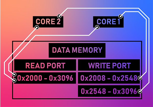
Our data memory used addresses 0x2000 to 0x3096. The first two bits are reserved for our counters as we discussed in the section above. The first half of the rest of the memory space is core 1’s write space. The second half of the rest of the memory space is core 2’s write space. And, both cores can read each others’ spaces.
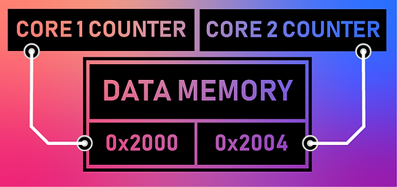
We also had to implement a method for determining if the information you are waiting for is ready, we created a counter-based implementation. By doing this, whenever a core would write a piece of information into the data memory its counter would increment. Our counter was stored in the shared data memory, and thus, could be referenced by any of the other cores. We would know if a core was out of date if their counters were not equal. The table on the right shows the location for each of the core’s counters.
To store important information - such as the core identification number - we decided to reserve important memory addresses in the private memory. Currently, we are only reserving the memory address 0x2000 within the private memory as the core ID. The core ID is set in hardware for each of the processors. Due to this, when creating an assembly program, this address should be read initially to determine which branch of code to execute (there should be a branch for each of the cores being used). During the process, we regularly cleared up our questions with the teaching team, which helped us get unstuck and continue making progress.
CHALLENGES
The most difficult part of building a dual-core processor was efficiently and effectively structuring our memory such that the two cores can “talk” to each other. Both cores shared data memory space, meaning each core had read access to all data memory registers. But, we needed to implement memory control such that each core only had write access to a position of the data memory. We tried to implement this by giving one core write access to the lower half and the other to the upper half.
Another challenge we faced was getting both cores to exit at the same time. Even after SYSCALL, random instructions would cause our final result to be inaccurate. We fixed this by implementing an AND gate with SYSCALL flags so that the system would exit if both cores are finished or when the condition is true.
OUR IMPLEMENTATION
To refer to our Verilog implementation, please use our GitHub repository linked here:
For the latest release, refer to:
Implementation instructions can be found in the readme:
Future Iterations
-
Add support for the full MIPS ISA
-
Test the processor with more number of specialized/unspecialized cores
-
Conduct CPU benchmarking to estimate the time advantage and power disadvantage of having multiple cores
-
Add a shared cache memory for interacting with the HDD/SSD
-
Make the memory indexing more robust by giving the control of defining the range of registers for loading and saving words to the software engineer, rather than implementing that in hardware
-
Create an actual mutual exclusion and semaphore specification, rather than blocking certain areas in the memory
-
Implementing a register file in between cores for more effective methods of communicating between cores than the current shared memory-based implementation